Offer of cooperation
1. Cross section analysis (SEM/Xe-PFIB/Ga-FIB).
During this process a local metallographic section is created with ion beam polished wall. This method allows to analyse the cross-sectional area of the object using SEM and Xe-PFIB/Ga-FIB. Those examinations are ideal for the investigation of quality of sinters, welds and multilayer structures, for example: integrated circuits or anti-reflective coatings.
2. 3D Reconstruction (SEM/Xe-PFIB/Ga-FIB).
Due to our advanced devices and professional software we are able to do visualization, analysis and 3D data presentation. Analysis of shape, volume, elemental composition and statistics of samples are achievable for R&D purposes.
3. Preparation of samples for Transmission Electron Microscopy (TEM).
In our laboratory we are able to prepare extremely thin samples (lamellae) intended for TEM. We guarantee the sample thickness below 100 nm, (depending on the material, thickness of the sample can be smaller than 20 nm). The lamellae are prepared from the area of the sample indicated by the customer and ready for TEM measurements. Moreover Xe-PFIB technology allows to create high quality samples aluminum or gallium based materials, what is impossible with Ga-FIB technology.
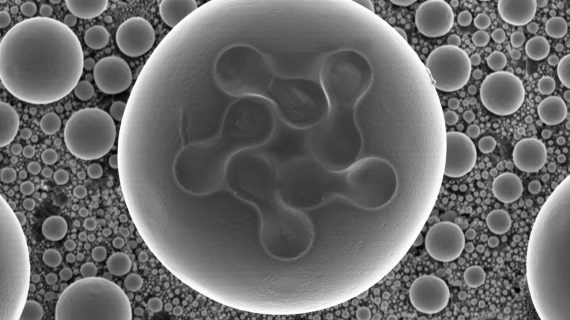
4. Surface analysis (SEM).
Research carried out using SEM can be used to verify shape, elemental composition of the materials in both micro and nano resolution.
5. Surface analysis (AFM).
Atomic Force Microscopy provides surfamay be used for verification of layer fabrication efficiency at any production stagece analysis which can detect the atomic scale differences of height. It is an ideal method to determine the roughness of the material surface and may be used for verification of layer fabrication efficiency at any production stage.
6. Deposition thin carbon films (High Vacuum Carbon Coater).
Our machine is ideal for deposition of thin, highly stable conductive carbon films. They are used for transmission and scanning electron microscopy (TEM, SEM).
7. Plasma/ultrasonic cleaning.
We offer cleaning with plasma and ultrasounds. Plasma cleaning is provided for removing nano-contamination from surface and allows to modify or improve the physical and chemical properties of the surface. Ultrasonic cleaning is mainly used for the surface of samples with complex shapes. The washing process is based on the cavitation phenomenon – small bubbles generated by high frequency pressure waves, implode on the surface of the object removing contamination.
8. Research planning.
We provide an assistance for planning a research and experiment program. Based on interviews with customers we will provide a research plan, to optimize service time and costs.
9. Prototyping.
Using our equipment, knowledge and experience we offer the services of prototyping structures for: micro- and nanoelectronics (NEMS and MEMS), micro- and nanofluidics, optical (photonic crystals, micro- and nanolens) and etc. 10. Aid in publications. If you are a researcher preparing your PhD thesis or other form of publication. We will be more than happy to aid you in preforming some minor research tasks free of charge.

Offer details:
Jakub Gawczyński
jakub.gawczynski@nanores.pl
Mecenasi Fundacji
Zostań mecenasem